Interconnect Is the Product: How AI Infrastructure Became a Networking Problem
Compute per accelerator has grown far faster than the bandwidth between accelerators, so on modern mixture-of-experts workloads the most expensive silicon in the building spends much of its time waiting on a wire. That imbalance is why the interconnect has become the real product being sold, why three incompatible scale-up fabrics are fighting for the same socket, and why a signal-integrity limit in copper is now dictating the physical shape of the data center.
Somewhere in a liquid-cooled rack, a token is waiting.
It reached layer 31 of a mixture-of-experts model about four hundred nanoseconds ago. The router looked at its hidden state, picked two experts out of a few hundred, and found that neither one lives on this accelerator. So the activation vector, a few kilobytes of bfloat16, has to leave the chip, cross whatever fabric the architects chose, land on two other accelerators, get processed, and come home before the layer can finish. Multiply that by every token in the batch, twice per MoE layer, across dozens of layers, and the accelerator that cost more than a house spends a good part of its time doing nothing at all.
That is the actual state of AI infrastructure in 2026, and it is the reason I think interconnect has quietly become the product rather than a component of it. We spent a decade making compute faster and a much shorter time making the wires between compute faster, and the gap finally got wide enough to matter more than the chip itself.
What follows is a tour of that gap: who is trying to close it, what they are betting, and which constraint is quietly deciding the answer for everyone. The rest of this follows the token.
Your accelerators are idle, and the wire is why
The imbalance is easiest to see in the ratios rather than the absolute numbers.
Between NVIDIA’s Blackwell and Rubin generations, per-GPU NVLink bandwidth doubles, from 1.8 TB/s to 3.6 TB/s. That is a genuinely enormous engineering achievement. It is also slower than the growth in floating-point throughput over the same interval, and much slower than the growth in the amount of communication that frontier model architectures demand. Every generation, the ratio of bytes moved to FLOPs available gets a little worse, and every generation the architects compensate by making the fast domain bigger.
Three workload changes turned this from an academic concern into the dominant design problem.
The first is mixture-of-experts. Dense models mostly need bandwidth for tensor and pipeline parallelism, which are relatively well-behaved traffic patterns with predictable partners. MoE introduces expert parallelism, where every token independently selects its own destinations, and the resulting dispatch and combine steps are all-to-all. All-to-all is the worst traffic pattern in networking: no locality, no reuse, and a completion time governed by the slowest path rather than the average one. A single straggler link stalls the entire collective.
The second is the shift in inference. Reasoning models generate long chains of intermediate tokens, so inference traffic started to look structurally like training traffic rather than like a lightweight forward pass. Serving them economically means large batches and wide expert parallelism, which means more all-to-all, not less.
The third is disaggregation. Splitting prefill and decode onto separate pools of accelerators is now standard practice for serving efficiency, because the two phases have opposite hardware appetites. But it means the KV cache has to move between pools, which puts multi-gigabyte transfers on the fabric that simply did not exist as a traffic class three years ago.
The industry didn’t choose to make interconnect interesting. The workloads forced the issue, and everyone is still catching up.
There’s an obvious objection to that framing: networking has always mattered in large clusters, and the industry has a long history of making bandwidth cheaper faster than workloads can consume it. That history doesn’t mean the current gap closes itself, or that interconnect vendors automatically capture the value sitting inside it. What’s different this time is that model architecture itself is starting to bend around fabric topology, which isn’t something that happened the last few times bandwidth got tight.
Before going further, one distinction has to be nailed down, because conflating these two things is the most common error in AI infrastructure design.
Scale-up is the fabric inside a coherent domain. Accelerators talk to each other with memory semantics, meaning loads and stores against remote memory rather than packets with headers. Bandwidth per accelerator runs to the terabytes per second. Latency is sub-microsecond and, more importantly, deterministic. The domain is bounded by physics and cost, not by protocol.
Scale-out is the fabric between domains. It is packet-based, it runs over Ethernet or InfiniBand, and it typically delivers between one and two orders of magnitude less bandwidth per accelerator. It scales to hundreds of thousands of endpoints, which scale-up cannot.
The design variable that matters is domain size. Every accelerator you can fit inside the scale-up domain is a chunk of tensor and expert parallel traffic that never touches the slow fabric. The industry’s fixation with domain size follows directly from that ratio, not from marketing.
It is also not free headroom. All-to-all traffic scales with the number of participants, so doubling the domain adds a proportional amount of dispatch-and-combine traffic that still has to land inside the same step time. Growing the domain is a bet that the fabric inside it can absorb the traffic the growth itself creates. For a wide MoE model, the difference between a 72-accelerator domain and a 1,024-accelerator one is the difference between an all-to-all that stays on a memory fabric and one that spills onto a packet network at a tenth of the bandwidth.
Our token’s fate is decided entirely by which side of that boundary its experts happen to live on.
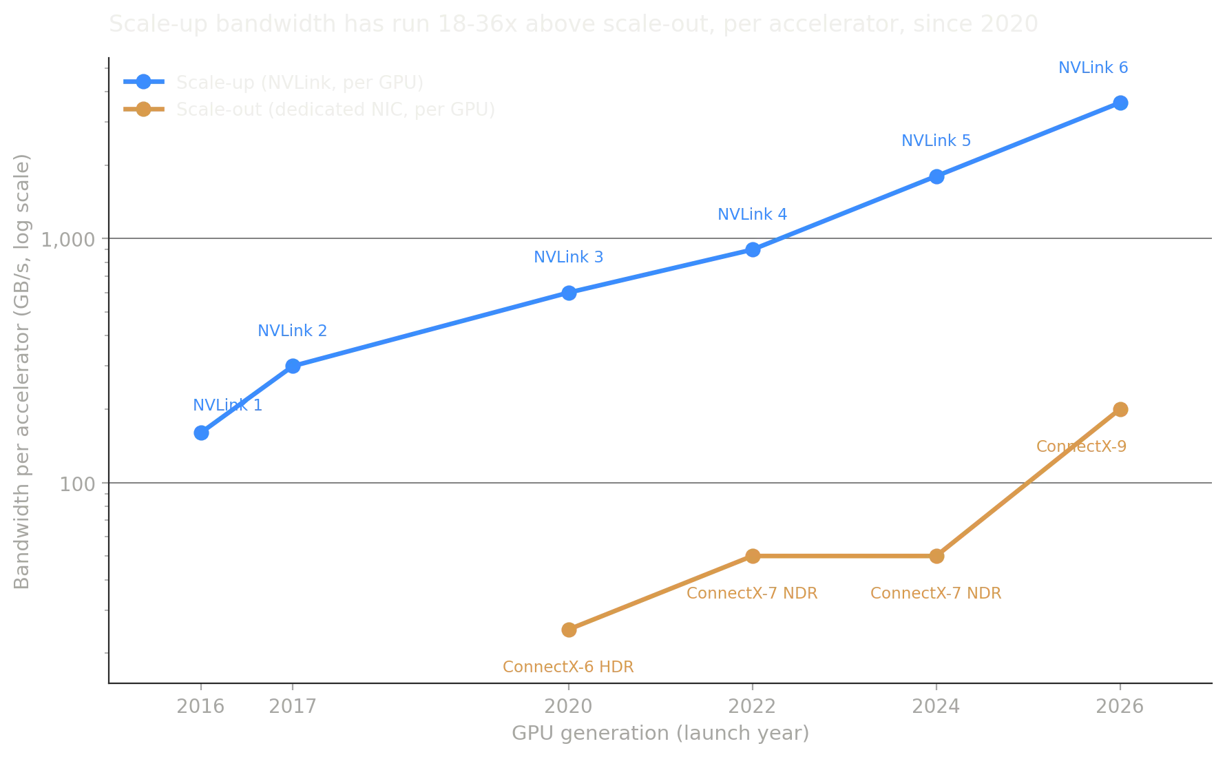
Fig 1. Per-accelerator bandwidth on NVIDIA’s scale-up fabric (NVLink) against the dedicated scale-out NIC bandwidth paired with the same GPU generation. The ratio isn’t perfectly smooth generation over generation, since NVLink and NIC standards upgrade on different cycles, but scale-up has run 18-36x above scale-out at every generation since NVIDIA standardized 1:1 NIC-per-GPU allocation at A100, and the absolute gap has grown roughly sixfold since 2020. (Sources: NVIDIA Pascal and Volta architecture whitepapers, NVIDIA NVLink, NVIDIA DGX A100 and DGX H100 datasheets, NVIDIA Rubin platform)
NVLink, UALink and Ultra Ethernet: the fabric that shipped beat the fabric that was ratified
If domain size is the prize, the fight is over who owns the fabric that defines it, and our token has no vote in the outcome. Whichever fabric its architects picked before the model ever trained decided how far its round trip home would be. There are three serious answers inside the domain, and they are not really competing on technology. They are competing on time and on control.
Scale-up: three answers, one deadline
NVIDIA’s answer is that the fabric should be memory, not networking. NVLink was never designed as a network in the way a network engineer would recognize. There is no packet header worth mentioning, no congestion control in the TCP sense, no software stack of any consequence in the data path. It is a memory fabric with a switch in the middle, and its entire design philosophy is that remote memory should behave as much like local memory as physics allows.
The workhorse today is still the GB200 NVL72: 72 Blackwell GPUs in one rack, 1.8 TB/s of NVLink per GPU, and roughly 130 TB/s of aggregate bandwidth inside the rack. The Rubin generation doubles per-GPU bandwidth to 3.6 TB/s and takes rack aggregate to around 260 TB/s. Rubin racks are in early deployment as I write this, first full VR200 NVL72 bring-up completed in June 2026, partner shipments from the autumn. These are specifications with silicon behind them, not a roadmap slide.
A small naming detail here is worth more than it looks. NVIDIA initially called the Rubin rack NVL144, counting the 144 compute dies across 72 packages, then reverted to VR200 NVL72 at CES 2026 to keep counting packages the way GB200 NVL72 did. Two dies per package, one name for the package. Anyone comparing domain sizes across vendors should check which unit is being counted, because the industry is not consistent about it and the difference is a factor of two in the headline number.
NVIDIA’s strategic move on top of this is NVLink Fusion, which opens the NVLink interface to silicon NVIDIA did not build, with Intel, Fujitsu, Qualcomm and SiFive among those signed up. Whoever owns the fabric owns the domain, and whoever owns the domain sets the terms.
The obvious pushback: owning infrastructure is also owning the capital risk of guessing wrong, and plenty of companies have built proprietary platforms that a cheaper open alternative made irrelevant a few years later. I’m not fully convinced NVLink Fusion escapes that fate, but the switching cost for a memory-semantic fabric is unusually high, which is exactly why NVIDIA is racing to sign up outside silicon before anyone has to pay it.
The consortium’s answer is that the fabric should be an open standard. UALink (Ultra Accelerator Link) 200G 1.0 was ratified in April 2025 with more than 85 member companies behind it, including AMD, AWS, Google, Intel, Meta, Microsoft and Apple. It runs 200 GT/s per lane, targets up to 1,024 accelerators in a pod, and preserves the thing that matters, which is memory semantics rather than packet semantics. It also makes a specific engineering argument that deserves respect: a smaller link-stack die area than the alternatives, which matters when every square millimeter on an accelerator is contested.
Broadcom’s answer is that we already have a fabric and it is called Ethernet. The Scale-Up Ethernet framework, published through OCP in April 2025, argues that the industry should stop inventing new link layers and instead strip Ethernet down for scale-up duty. The silicon behind that argument is Tomahawk 6, a 102.4 Tbps single-chip switch supporting 512 ports at 200G, with both copper and co-packaged optics variants. It began shipping in June 2025 and reached production volume in March 2026, going from first samples to volume in under three quarters.
Here is the detail that breaks the tidy version of this story, and it has only sharpened since. In April 2026 the consortium ratified UALink 2.0, adding in-network compute, a chiplet definition, and a physical-layer split that opens a path to 400G per lane. It is a genuinely good second specification. It was also published before any UALink 1.0 silicon shipped. First hardware from AMD, Intel and Astera Labs is expected late in 2026, with production systems in 2027.
So the scoreboard reads: the open standard is two specifications ahead, and the merchant Ethernet silicon is in volume production across more than 100,000 XPUs. Standards bodies ship documents on their own schedule. Buyers cannot install a document.
The practical outcome is that scale-up is consolidating into two camps rather than three: NVIDIA’s memory fabric for people buying NVIDIA systems, and Ethernet-derived fabrics for everyone building custom silicon. UALink’s most likely future isn’t as a loser but as a set of good ideas the Ethernet camp absorbs, which is the usual fate of a good standard that arrives late.
Side by side, the three bets look like this. Note the unit mismatch in the bandwidth row, which is itself part of the story: NVIDIA quotes bandwidth per accelerator, UALink quotes it per lane, and Ethernet quotes switch capacity. Comparing these three numbers directly is a category error that vendor marketing is happy to let you make.
| Attribute | NVLink 6 | UALink 200G 1.0 | Scale-Up Ethernet |
|---|---|---|---|
| Semantics | Memory, load/store | Memory, load/store | Packet |
| Bandwidth | 3.6 TB/s per GPU | 200 GT/s per lane | Switch capacity, 102.4 Tbps on Tomahawk 6 |
| Stated max domain | 576 GPUs at the NVLink 5 generation | 1,024 accelerators per pod | Not bounded by the spec |
| Switch silicon | NVSwitch. Rubin racks in early deployment, partner shipments from autumn 2026 | No 1.0 silicon shipped yet. First hardware late 2026, systems 2027 | Tomahawk 6, production volume since March 2026 |
| Governance | Proprietary, third-party attach via NVLink Fusion | Open, 85+ member consortium | Open framework published through OCP |
Fig 2. The three scale-up fabrics on the attributes that decide a purchase. The bandwidth row is deliberately not like-for-like: each vendor quotes the unit that flatters it, so read the unit before comparing the number. (Sources: UALink 200G 1.0, NVIDIA Rubin platform, Broadcom Tomahawk 6)
Scale-out: the wire was never the problem, the transport was
When the token’s expert lives outside the domain, it leaves the memory fabric and enters a packet network, and everything changes: bandwidth drops by one to two orders of magnitude, latency becomes a distribution rather than a number, and software gets involved.
For years the answer here was RDMA over Converged Ethernet, and for years it was a slightly uncomfortable answer. RoCE inherited an assumption from InfiniBand that the network is lossless, which it enforces with priority flow control. PFC works until it does not, and its failure modes at scale are genuinely unpleasant: head-of-line blocking, congestion trees that propagate backward through the fabric, and the occasional deadlock. Anyone who has operated a large RoCE fabric has a story about a single misbehaving host taking down a pod.
Ultra Ethernet Specification 1.0, released in June 2025 by the Ultra Ethernet Consortium (UEC), is the industry’s attempt to fix this properly rather than incrementally. It runs to more than 560 pages, and the important thing about it is that most of those pages are not about the physical layer at all. The wire was never the problem. The transport was.
Ultra Ethernet Transport changes the assumptions that made RoCE fragile. It sprays packets across all available paths rather than pinning a flow to one via hashing, which is the single biggest fix, because ECMP hash collisions on a handful of enormous elephant flows is precisely the pathology that wrecks AI fabric utilization. It permits out-of-order delivery and reassembles above the transport, which is what makes spraying viable. It replaces the lossless assumption with congestion control designed for incast, and defines an RDMA API that does not require the network to be perfect.
The port-speed numbers matter less than what UET actually fixes. “Ethernet versus InfiniBand” has always been the wrong framing here: the real question is whether a transport built for many small independent flows can be adapted to a workload made of a few gigantic synchronized ones. UEC’s answer is that it couldn’t be adapted; it had to be rebuilt, and the rebuild is what shipped.
InfiniBand is not going away, and NVIDIA continues to invest in it heavily. But its historical advantage was that it had a transport built for this traffic while Ethernet did not, and that advantage now has an expiration date. I don’t know exactly how long that expiration date is, but the trend line already points one direction.
It is worth being precise about what NVLink versus InfiniBand actually means, because the two get compared as though they were alternatives. They are not. NVLink is the scale-up fabric inside the domain and InfiniBand is one option for the scale-out fabric between domains, so a large NVIDIA cluster typically runs both at once. The real competition is NVLink against UALink and Scale-Up Ethernet on one tier, and InfiniBand against Ultra Ethernet on the other.
Google, Amazon and OpenAI skipped the menu and built their own fabric
The most interesting architectures in this space belong to the organizations that looked at the menu in the previous section and walked away.
Google made the topology reconfigurable, and did it before the argument started. The TPU fabric does not look like anything else in production. Chips connect over Inter-Chip Interconnect in a 3D torus rather than a switched fat tree, with a rack forming a 64-chip cube. Cubes then connect through Apollo, an all-optical circuit switch, and Ironwood scales that to 9,216 chips in a superpod, with 9.6 Tb/s of ICI bandwidth per chip and 1.77 PB of shared HBM across the pod.
The optical circuit switch is the part worth studying. An OCS does not inspect packets. It physically steers light from an input port to an output port using microelectromechanical mirrors, which means it consumes almost no power relative to a packet switch, adds almost no latency, and is completely agnostic to data rate. Upgrade the transceivers on both ends and the same switch carries the higher rate, which is an unusually good property in an industry that replaces switch silicon every two years.
What you give up is packet switching. A circuit must be established before traffic flows, so this only works when traffic patterns are known ahead of time and stable for a while. For synchronous training on a torus, they are. Google gets topology it can reconfigure per job, failure isolation where a dead cube is routed around rather than fragmenting the pod, and a switching layer that outlives the generation. The catch is scheduling. Google can make this work because it controls the entire stack top to bottom; I wouldn’t assume the same architecture transfers cleanly to a general-purpose cloud operator, which is probably why nobody has copied a design that’s been in production since TPU v4.
Amazon built a scale-up domain and skipped the rack constraint. The Trainium3 UltraServer puts 144 chips into a single scale-up domain, assembled from 36 servers of four chips each, connected by NeuronLink v4 through a two-tier arrangement of NeuronSwitch silicon. The topology is all-to-all, chosen explicitly for MoE and low-latency collectives, and it spans the printed circuit board, the backplane, and cross-rack connections.
That last detail is the interesting one. By treating cross-rack as a first-class part of the scale-up domain rather than the boundary where scale-up ends, Amazon gets a 144-chip domain without needing to win the density race inside a single rack. Different constraint, different answer, and a preview of the wall the next section is about to hit: extending a memory-semantic domain across racks means extending the electrical channel too, and that channel does not extend for free.
Then Amazon walked part of the way back to the menu. Trainium4, due late 2026 or early 2027, will support NVLink Fusion inside NVIDIA MGX racks while keeping UALink for its own UltraServer designs. A founding UALink member, with its own accelerator and its own switch silicon, still chose to attach to NVIDIA’s fabric for one of its two rack architectures. What it buys is the rack, tray, cooling and power envelope the industry is already tooled for.
That is NVLink Fusion working exactly as designed. You do not have to beat a competitor’s accelerator if their accelerator plugs into your fabric.
OpenAI decided the fabric was worth owning outright. The 10 gigawatt collaboration with Broadcom, announced in October 2025, with deployments beginning in the current half and running through 2029, is not primarily a chip deal. Read the wording: the racks are scaled with Ethernet and connectivity from Broadcom, meaning the scale-up fabric and the scale-out fabric are both Ethernet, both from the same vendor, and both under the design control of the company that owns the models.
To me, the more interesting part of the OpenAI-Broadcom relationship isn’t the silicon. It’s the decision to control the fabric too. Vertical integration into silicon is usually a story about margin. Owning the interconnect is a different bet: it says OpenAI thinks the fabric itself decides which model architectures are trainable, not just which ones are cheap.
The money involved is not a rounding error on the compute bill. Dell’Oro Group forecasts that cumulative spending on switches in AI back-end networks will approach $1 trillion between 2026 and 2030, and expects scale-up to account for more than half of that market by 2030. Read that second clause again. The tier that did not exist as a distinct market five years ago is forecast to outgrow the one everybody has been building for a decade.
None of the three care about switches for their own sake. Whoever controls the path the token takes controls what the next model can look like, and none of them wanted that decision sitting on someone else’s roadmap.
Copper ran out of road at 224G, and it redesigned the building
Now follow the token down instead of out, past the protocol arguments, into the physical layer. This is where the constraint that actually determines the shape of the data center lives, and it is not a compute constraint.
Serial links are at 224 Gbps per lane. Getting there required PAM4 signaling, aggressive equalization, and forward error correction, and each of those costs power and latency. But the binding problem is reach.
At 112G, a passive copper cable could run roughly two to two and a half meters. At 224G, that collapses to about a meter for a standard passive channel. Marvell markets a long-reach 224G SerDes that drives 2.5 meter copper channels at 1e-11 BER, and the fact that this is a headline feature tells you how tight the budget has become.
A meter is not an abstraction. It is a physical dimension in a building.
The scale-up domain is roughly the size of one rack because that is how far a 224G signal travels in copper. Ask an architect why 72 and you will get an answer about tensor parallelism, which is a rationalization arrived at afterward. The domain got the shape signal integrity allowed, and parallelism strategies, expert counts and rack SKUs were all fitted to that shape once it was fixed.
Follow that constraint outward and most of the modern data center falls out of it. If the domain must fit in a rack, the accelerators must be dense. If they are dense, the rack is drawing tens of kilowatts and heading toward hundreds. If it is drawing that much power in that volume, air cooling is finished and you are plumbing liquid to every rack. If you are plumbing liquid, you are rebuilding the facility, not the row.
Liquid cooling is usually explained as a consequence of chip power. It is at least as much a consequence of copper reach, because copper reach is what forced the density in the first place.
The rest of the physical layer is a set of increasingly elaborate workarounds for the same wall. Retimers regenerate the signal partway along the channel, at the cost of power, latency and another component that can fail. Active electrical cables put the retiming in the cable itself. Flyover cabling bypasses the PCB entirely, because at 224G Nyquist frequencies a few inches of unremarkable circuit board becomes a meaningful loss budget, so designers route signals over cable rather than through the board they just paid to fabricate.
Meanwhile PCIe 7.0 is specified, with devices expected around 2027, doubling again to 128 GT/s. It faces exactly the same physics.
Every one of these techniques buys a little more electrical margin, usually measured in centimeters. The next SerDes generation will spend that margin again. I don’t see a path for copper to remain the dominant medium at these distances, and at some point the fight stops being about a better electrical channel and starts being about removing the electrical channel entirely.
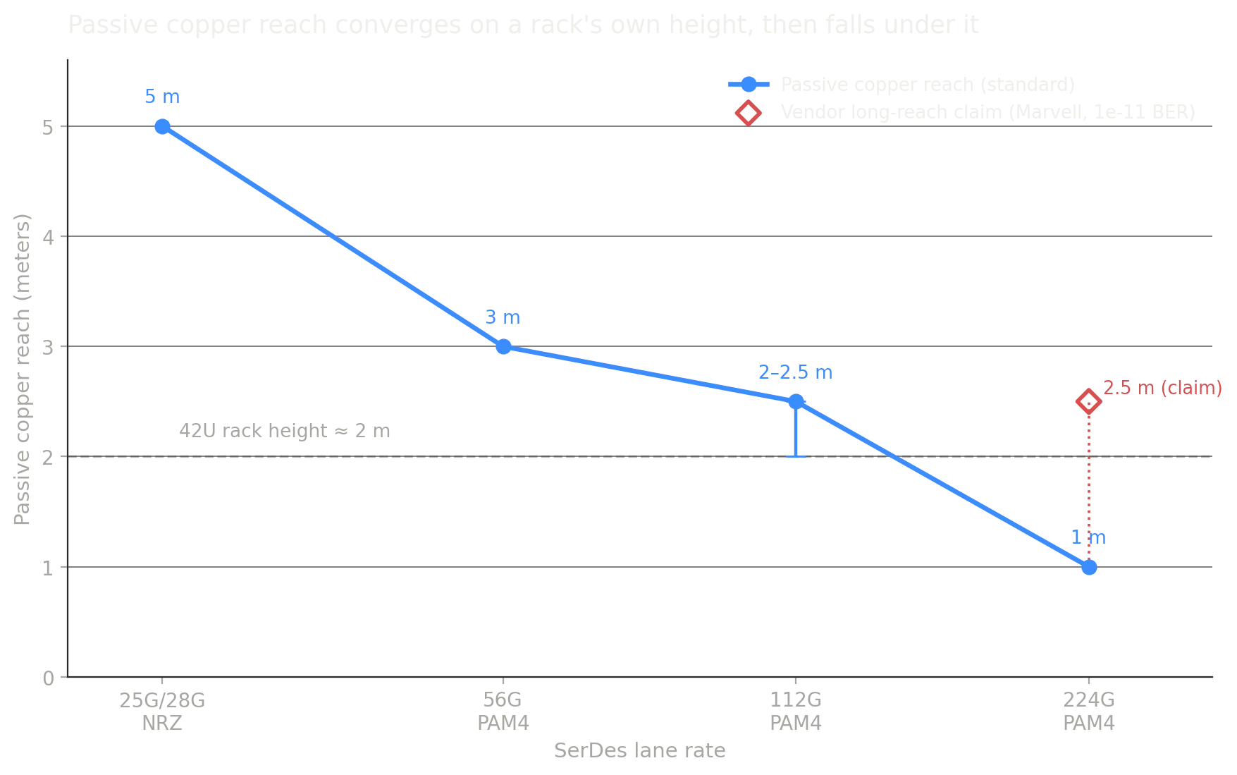
Fig 3. Passive copper reach collapses as SerDes lane rate climbs, and by 112G it has converged on a standard rack’s own height. That is not a coincidence the industry designed toward; it is a constraint the industry designed around. (Sources: IEEE 802.3by-2016 [25GBASE-CR], IEEE 802.3cd-2018 [200GBASE-CR4], Synopsys, 224G SerDes IP and linear-drive optics, Marvell, 224G long-range SerDes)
Optics moved into the package, and the argument became about repair
Copper’s meter is a hard limit on copper, not on the industry. The obvious response is optics, which has been available for decades and does not care how far it has to travel. The reason it did not simply replace copper already is that pluggable transceivers, the little modules in the switch faceplate, are expensive in the one currency that now matters most.
A pluggable optic burns roughly 15 to 20 picojoules per bit. Co-packaged optics, where the silicon photonics sit on the same substrate as the switch ASIC instead of at the end of a copper trace, brings that toward 5 pJ/bit or below. At the scale of a facility moving hundreds of terabits, a factor of three or four in pJ/bit stops being an efficiency statistic and becomes an allocation decision: watts spent moving data are watts not spent computing on it.
Put the two numbers side by side, and the gap is not the only thing that matters. So is what kind of number each one is: one is a measured range, the other is a vendor-stated ceiling with no published floor.
| Metric | Pluggable optics (DSP) | Co-packaged optics |
|---|---|---|
| Energy per bit | 15-20 pJ/bit (measured range) | under 5 pJ/bit (vendor-stated upper bound, no published floor) |
| Optical I/O power at 400 Tb/s* | 6-8 kW (computed) | ≤2 kW (computed) |
Fig 4. Pluggable optics measure 15-20 pJ/bit across multiple sources. Co-packaged optics is reported only as “under 5 pJ/bit,” an upper bound with no published floor, which is why the table states it as a ceiling rather than collapsing it to a single point estimate or a range down to zero. The kilowatt row is computed, not independently sourced: pJ/bit × NVIDIA’s own stated Spectrum-X Photonics aggregate throughput of 400 Tb/s, and that throughput is for one switch, since a real fabric runs hundreds of them. That gap, at a single switch, is why this is a power-allocation decision rather than a performance footnote. (Sources: Marvell, Silicon Photonics Light Engine for Low-Power, Rack-Scale Interconnect; throughput figure from NVIDIA Spectrum-X Photonics, already cited in this article)
Most commentary reads this as a bandwidth story. It is not. Pluggables can carry the bandwidth perfectly well. Optics is moving into the package because the electrical channel between the switch chip and the faceplate became the most expensive real estate in the system, measured in watts, and shortening that channel to nearly zero is the entire value proposition.
The products are not roadmap items any more. NVIDIA’s Quantum-X Photonics offers 144 ports of 800 Gb/s InfiniBand with liquid cooling for the onboard photonics, and went into production deployment alongside GB300 racks in mid-2026. Spectrum-X Photonics, the Ethernet side, scales to 512 ports of 800 Gb/s for 400 Tb/s of throughput and is arriving now. NVIDIA claims 3.5x better power efficiency and 4x fewer lasers than pluggable equivalents. Broadcom’s Tomahawk 6 Davisson pairs 102.4 Tbps of switching with co-packaged optics in a single package. Treat vendor efficiency multipliers as vendor claims, but the direction is not in dispute.
So why is CPO not yet the default?
Because of a question that has nothing to do with physics: what happens when a laser dies?
A pluggable optic that fails is a two-minute repair by a technician who does not need to know what the switch does. A co-packaged optic that fails is attached to a switch ASIC worth many thousands of dollars, in a liquid-cooled sled, and the failure domain is now the whole package. Operators run on service-level agreements and mean-time-to-repair, and CPO changes both in ways their existing procedures do not cover. The industry’s mitigation is external laser sources, so the least reliable component stays field-replaceable while the modulators and detectors move into the package.
The pace of adoption is therefore set by RMA models, spares strategy and warranty terms rather than by pJ/bit. The physics got solved a while ago. What’s still being fought over is who eats the cost when a laser fails inside a package worth five figures. Watch which operators sign first. They are the ones who decided the power saving outweighs a repair procedure they have never run.
This rhymes with the space power infrastructure survey: in both domains the interesting engineering is not peak capability but the joules spent moving a unit of something useful, and in both, systems designed as isolated islands hit a wall once they must interoperate at scale.
The next constraint to break is the rack boundary itself
Our token has now traveled about a meter, and everything above was an argument about that meter. Here is where the next few years take it.
Optics moves from the switch into the accelerator package. Co-packaged optics on switch silicon is the easy case, because a switch is a networking product sold to people who accept networking failure modes. Putting optical I/O on the accelerator itself is harder and more valuable, because it decouples domain size from copper reach entirely. When an accelerator’s links leave the package as light, the one-meter constraint that currently defines the rack dissolves, and the scale-up domain can be as large as the coherence protocol and the failure model allow.
The mechanism for that already exists. Ayar Labs builds TeraPHY as a UCIe optical chiplet at 8 Tbps bidirectional, which turns optical I/O into a block you drop into someone else’s package rather than a capability you have to build. Lightmatter takes the interposer route with Passage, putting optical circuit switching into the substrate itself. And in February 2026 Marvell closed its acquisition of Celestial AI, which is the more telling data point: merchant silicon vendors don’t buy photonic startups outright unless they’ve already decided optical I/O belongs in the product, not bolted onto it.
Memory semantics keep winning over packet semantics inside the domain. Every serious scale-up design has converged on loads and stores rather than send and receive, because software that must explicitly marshal a message cannot hide microseconds the way hardware coherence can. Expect the boundary between “remote memory” and “the network” to keep blurring, and expect that to be where the hardest reliability problems concentrate, since memory semantics offer far fewer places to hide a retry.
Scale-across becomes an accepted third tier. Single sites are running into grid interconnection limits before they run into technical ones, so training across buildings and across metro distances stops being exotic. That introduces a tier with millisecond-scale latency, and it’s not yet clear which collectives can tolerate it or how much of the parallelism strategy has to bend to keep them off the long path.
Model architecture starts getting designed around fabric topology. Expert counts, routing top-k, and the granularity of tensor parallelism are already chosen partly for what the interconnect can sustain. That causality is likely to keep flipping: instead of building fabrics to fit whatever architecture researchers invent, researchers will increasingly invent architectures that fit the fabrics already on the floor.
Four trends are easy to agree with and hard to attach a date to. Here are the three I would actually bet on.
Two bets
-
Scale-up switching outsells scale-out switching before the end of 2028, because domain-size competition pulls spending forward faster than scale-out port growth does. I expect to be wrong here on timing rather than direction: pulling a forecast in by two years assumes a spending pattern that supply constraints could easily stretch back out.
-
At least one major operator publicly reports a multi-week outage or capacity loss caused by a fabric-layer failure rather than a compute or power failure. As domains get larger and their semantics get more memory-like, the blast radius of an interconnect fault grows faster than the tooling to contain it.
The wire was always the computer
The token finally reaches its expert, gets multiplied by a matrix that a person spent months tuning, and comes home to be recombined. Total round trip: a few microseconds if it stayed inside the domain, considerably more if it did not. Repeat a few trillion times and you have a trained model.
The industry spent a decade optimizing what happens at the destination. The next decade belongs to whoever optimizes the journey, because that is where the time is now going, and time on this equipment is the only thing anybody is actually buying.
Interconnect might not stay the top constraint. Power and cooling could just as easily reclaim that position within a few years, and I’d rather flag that risk than pretend this framing is permanent.
The uncomfortable implication for anyone specifying infrastructure: the accelerator on the datasheet is no longer the thing you are choosing. You are choosing a domain size, a failure model, and a repair procedure, and those three decisions will determine what you can train long after the FLOPs number has stopped being interesting.
So when you next evaluate a cluster, try asking a different question than how fast the chips are. Ask how far a signal can travel before it has to become light, and who has to be on site when that light goes out.
References
- UALink Consortium, Ultra Accelerator Link 200G 1.0 Specification, April 2025
- The Register, UALink delivers 2.0 spec before v1.0 silicon ships, April 2026
- Broadcom, Tomahawk 6 shipping in production volume, March 2026
- NVIDIA, AWS integrates AI infrastructure with NVLink Fusion for Trainium4
- Ayar Labs, first UCIe optical chiplet for AI scale-up architectures
- Lightmatter, Passage co-packaged optics at 1.6 Tbps per fiber, March 2026
- Ultra Ethernet Consortium, Specification 1.0, June 2025
- Broadcom, Tomahawk 6 102.4 Tbps switch, June 2025
- Broadcom, Tomahawk 6 Davisson with co-packaged optics
- NVIDIA, Inside the Vera Rubin platform
- NVIDIA, NVLink as the scale-up network for AI factories
- NVIDIA, Spectrum-X Photonics co-packaged optics switches
- Google Cloud, Inside the Ironwood TPU codesigned AI stack
- AWS, Trainium3 UltraServer
- OpenAI and Broadcom, 10 gigawatt accelerator collaboration, October 2025
- Synopsys, 224G SerDes and linear drive optics
- Marvell, 224G long-range SerDes for scale-up
- PCI-SIG, PCI Express 7.0 specification release
- Dell’Oro Group, AI back-end switch sales to approach $1 trillion over the next five years